Precision and purity are crucial in chip production.

Precision and purity are crucial in chip production.

Chemistry is expanding the chip industry

Readingtime 8 minutes

Microchips are scarce worldwide, and manufacturers are working to create large new production facilities. Evonik is helping industry achieve its goals by supplying it with high-class silanes and hydrogen peroxide

publication date17th March 2023

TEXTNorbert Kuls & Tom Rademacher

Tom Rademacher is a freelance journalist based in Cologne, Germany. He writes about scientific and industrial topics, among others
Norbert Kuls is Evonik’s Communications Manager in North America and a former US correspondent for German newspapers

Allentown, Pennsylvania, and Portland, Oregon, are almost 4,500 kilometers apart. At the end of September, Dr. Purnima Ruberu made the long trip from the Evonik facility in the east of the United States to the city near the Pacific coast. Her destination was the International Conference on Planarization Technology, or ICPT for short, which brings together companies and experts from all over the world. For three days, the participants focused on the microscopically precise polishing of semiconductors—a highly specialized industry that holds great significance. Evonik wants to enter this market, and Ruberu has the key.

“The ICPT is an important event for the industry—and Portland is an important place,” she says. There is a bustling semiconductor industry in the “Silicon Forest” that surrounds the city. Intel alone—the world’s second-largest chip producer after the Korean market leader Samsung—employs more than 20,000 people in the region. Taiwan’s TSMC comes in third. The conference was held at just the right time. It offered the participants an opportunity to take stock of the situation for the first time since the forced pause caused by the pandemic, and right in the midst of the global chip crisis. Ruberu, who heads applications research for silanes in the semiconductor industry at Evonik, added a few more days to her stay to meet experts, visit potential customers, and tour a production facility in Portland. “Things are really kicking off,” she says.

Evonik researcher Purnima Ruberu has opened up a completely new business for the company with a silica based on the so-called Stöber process

A race is on in the chip industry. One of the main reasons for this is the continuing supply bottlenecks for microprocessors, which threatened to stall the post-pandemic economic recovery in many places last year. Lots of developments had come to a head. During the pandemic, many people digitally upgraded their home offices while streaming services and video conferencing providers expanded their server farms. Microsoft and Sony launched new game consoles at the same time and ordered large quantities of chips in advance. Moreover, the boom in cryptocurrencies consumed processor capacity. And all of this happened while virtually every supply chain worldwide was stalled by the coronavirus pandemic and geopolitical conflicts.

BILLIONS FOR MORE INDEPENDENCE

Around 80 percent of the world’s microchips are currently produced in Asia. Like Europe, the USA is desperate to reduce its dependence on foreign suppliers and wants to add more links to its domestic semiconductor supply chain. The latest boost came this year from President Joe Biden with the CHIPS and Science Act, a national investment program worth around $280 billion. The European Union also wants to promote its domestic chip industry more strongly—with the European Chips Act, which has a volume of €43 billion.

ELEMENTS Newsletter
Get fascinating insights into the research Evonik is conducting, and its social relevance, by subscribing to our free newsletter.

The consequences of the chip shortage can be felt far and wide because processors are now found in almost everything. Two out of three companies in Germany import digital components, according to a survey by the industry association Bitkom. If the supply falters, the effects are correspondingly drastic. This was particularly evident in the automotive industry. At Volkswagen, for example, production was halted for weeks in 2021 due to a shortage of semiconductors. However, this situation also harbors opportunities. Chipmakers and their suppliers are open to new ideas as they try to counteract this problem, create additional capacity, and broaden the supplier base. Purnima Ruberu experienced this in Portland. “Many more doors are opening for us compared to just a few years ago,” she says.

As a specialty chemicals company, Evonik supplies a whole series of solutions for microchip production. Demand for new materials is growing, partly because the chips are getting smaller and smaller. Today the company’s palette ranges from special cleaning agents and precursor products for polishing to material components for individual semiconductor layers.

Silanes play an especially important role. Silanes are molecules that have a silicon atom at their core. Like the legs of a spider, various other functional groups are connected to this central atom. Evonik produces silanes for a variety of applications, such as coatings, sealants, and optical fibers. In chip manufacturing, the “legs” of the silane play a secondary role; the silicon in the core is the key. For example, chlorosilanes are used to produce silicon monocrystals known as ingots that are up to 30 centimeters thick and two meters long. Cut into round ultra-fine wafers, they form the basis for every modern microprocessor.

From lab to industry: All the samples are created in Allentown’s Innovation Center. Now Purnima Ruberu is working on getting the first plant up and running for commercial production

From lab to industry: All the samples are created in Allentown’s Innovation Center. Now Purnima Ruberu is working on getting the first plant up and running for commercial production

Another product called tetraethoxysilane, TEOS for short, serves in later processing steps as a sort of silicon cab that can be used to apply ultrafine insulating layers. For this purpose, TEOS is applied to the wafer using a process called chemical vapor deposition (CVD). The attached ethyl groups are then reacted off at high temperatures, which means the “legs” are removed from the TEOS. What remains is a body of silicon dioxide. The fused quartz-like coating that is formed is just a few nanometers thick.

Evonik produces TEOS in more than a dozen grades of purity. For the CVD process, however, only the highest grades are wanted. Even the smallest traces of foreign metals would cause defects in the final chip. This effect is even more pronounced in the production of five-nanometer-class chips, let alone the latest three-nanometer class. For TEOS, Evonik therefore controls the absence of metallic impurities down to the parts per trillion range. “You can think of it as trying to find a sugar cube in a reservoir,” says Matthias Abele, the head of quality control at the Silanes business line. Abele supervises the company’s purity standards from the Evonik site in Rheinfelden, Germany. Situated on the border with Switzerland, this location houses the reference laboratory for the company’s silane division.

“Many more doors are opening for us compared to just a few years ago”

PURNIMA RUBERU, HEAD OF APPLICATIONS RESEARCH FOR SILANES IN THE SEMICONDUCTOR INDUSTRY

In the hunt for impurity atoms, Abele’s team uses elemental trace analysis techniques such as inductively coupled plasma mass spectrometry (ICP-MS)—“measuring homeopathic concentrations,” as Abele jokingly calls it. Evonik ensures reproducible and reliable results through interlaboratory tests, in which the same sample is also analyzed in the company’s laboratories in Belgium, China, and the USA.

A STARTUP WITHIN THE COMPANY

The highest purity and uniform quality are also a concern for Purnima Ruberu, who studied chemistry at the University of Colombo in her native Sri Lanka. After graduating she came to the USA to earn her doctorate at Iowa State University, then worked in Texas as a senior researcher at two tech startups in the semiconductor and electronics industries. In 2018 Evonik recruited her for the Allentown location as an expert in the production of nanostructures for the semiconductor industry. Ruberu became the preferred candidate not only because of her professional expertise. Her experience with young and fast-moving technology companies also played an important role. “It was all about building a startup within Evonik,” she says. Since then, Ruberu has set up a dedicated development laboratory for abrasive particles for semiconductor manufacturing at the Allentown location, which this year became one of Evonik’s global competency centers. This lab creates new solutions for further processing steps in chip production.

The first innovation aims to achieve absolute precision in polishing. Some modern microchips consist of more than 100 ultrafine layers. Virtually every layer is etched, patterned, and polished after application. Chemical mechanical planarization (CMP) achieves surface specifications that must be precise within one nanometer. The polishing agent consists of slurry, a milky suspension containing an abrasive and a chemically aggressive component. The material of choice is silicon dioxide, also known as silica.

That’s fine: Nanoparticles of silica float in a milky dispersion. They are perfectly suited as abrasives for microprocessors

Evonik is one of the world’s leading producers of silica. This simple molecule, which consists of one silicon atom and two oxygen atoms, occurs in nature primarily in crystalline form as quartz. For polishing semiconductors, the industry relies on colloidal silica. This consists of extremely small, round silica particles that float as a suspension in water or another solvent. Evonik produces colloidal silica using the Stöber process. Back in 1967, the German scientist Werner Stöber and two colleagues described in a technical journal how they had produced particularly round and uniform silica particles by means of the hydrolysis of alkyl silicates with ammonia as a catalyst and subsequent condensation. Purnima Ruberu uses this process along with ­Evonik’s TEOS, which serves as the starting material. “The idea had already been floating around in the company for a while,” she says.

With the purchase of the US company Silbond in 2014, Evonik acquired not only its TEOS business and its Allentown location but also some fundamental patents for this process. “However, it was a long road from there to a process ready for practical application,” Ruberu says. The process she and her team perfected over three years of laboratory and pilot-scale work now makes it possible to produce particles as small as twelve nanometers. By comparison, human hair is about 6,000 times as thick. “But the main thing is that these peanut-shaped particles we produce are extremely uniform in size and shape,” Ruberu explains.

Experienced and equipped: The former fab process engineer Laura Ledenbach stands in front of special storage tanks filled with high-purity hydrogen peroxide in Bayport. Chipmakers need vast amounts of this cleaning chemical.

Experienced and equipped: The former fab process engineer Laura Ledenbach stands in front of special storage tanks filled with high-purity hydrogen peroxide in Bayport. Chipmakers need vast amounts of this cleaning chemical.

When used as abrasives in slurry, these particles can achieve exact surface specifications. The silane-based process also has another advantage over the current standard process, in which silica is obtained by ion exchange from water glass, i.e. sodium or potassium silicate. Water glass-based colloidal silica is comparatively easy and inexpensive to produce. But even the tiniest remnants of some alkali metals pose a significant problem for microprocessor manufacturers. “We control our process diligently to minimize unwanted metal contamination,” Ruberu says.

CLEANER THAN A HOSPITAL OPERATING ROOM

Evonik’s first test facility for colloidal silica is in Allentown and consists of a tangle of tubes and glass reactors. The associated pilot plant already supplies enough material for customer samples, which slurry manufacturers use to test new polish formulations. Evonik is in discussions with four of the six leading companies in this sector. With input from Ruberu’s technical team, the Silanes business line has now designed its first commercial plant for this product. The plan is to deliver quantities of up to several tons within next couple of years.

“H2O2 touches every microchip on every wafer in every fab around the world”

Laura Ledenbach, Head of the global industry team for electronics at the Active Oxygens business line

Silica is not the only specialty chemical with tremendous growth potential that Evonik supplies to semiconductor manufacturers. The company also ranks among the world’s top suppliers of hydrogen peroxide (H2O2) for the electronics industry. Hydrogen peroxide, which comes in different purity grades, is widely known as a powerful yet environmentally benign disinfectant and cleaning agent. This is because, after its powerful oxidative action, hydrogen peroxide breaks down into nothing more than oxygen and water—leaving no harmful residues in the environment. These “green” properties benefit a number of industries. Pulp and paper producers, for example, use hydrogen peroxide as a bleaching chemical and to remove printing ink in the recycling process.

Semiconductor manufacturers use hydrogen peroxide as a crucial cleaning agent in their fabrication plants—“fabs” in industry parlance. It also serves as an oxidizing agent in slurries for planarization (CMP). For the electronics market, Evonik supplies the chemical in two grades: a “pre-electronic” grade goes to companies that further purify it. Evonik is, in fact, the dominant player in North America for this important market, with years of experience serving the industry from its plants in the USA and Canada. But the company also produces and directly sells high-purity grade hydrogen peroxide to semiconductor clients.

Under control: The operator Anthony Castillo walking among tanks and pipes in Evonik’s hydrogen peroxide facility in Bayport, south of Houston

Chipmakers need vast quantities of hydrogen peroxide. It is the second-most used chemical in semiconductor production after ultrapure water. “It touches every microchip on every wafer in every fab around the world,” says the quality manager Laura Ledenbach, head of the Global Industry Team for electronics at Evonik’s Active Oxygens business line. As chipmakers become more advanced and the chips get smaller and smaller, they increasingly need to avoid contamination. The leading, cutting-edge players in the industry can’t afford to let anything hamper their manufacturing process. “That’s why everyone is covered from head to toe, dressed in a bunny suit, and wearing hairnets and gloves,” Ledenbach says. Employees in semiconductor plants are prohibited from wearing make-up, perfume, or any jewelry or metal. “A fab is cleaner than a hospital operating room,” she explains.

Ledenbach wore those bunny suits herself when she worked in fabs as a process engineer earlier in her career. This engineering experience now helps her understand and anticipate the needs of Evonik’s semiconductor clients. “The crucial element is consistency,” she says. “Our customers want to receive the same high-quality product throughout the year—24/7.”

A hard hat with a Texas flag: Evonik employee Alex Romero collects a high-purity hydrogen peroxide sample from the storage tanks in Bayport

A hard hat with a Texas flag: Evonik employee Alex Romero collects a high-purity hydrogen peroxide sample from the storage tanks in Bayport

A VERY HIGH-VALUE BUSINESS

Evonik produces hydrogen peroxide for the electronics industry in multiple plants around the world. High-purity hydrogen peroxide is a very regional product. To avoid the risk of contamination during transportation and to ensure supply security, Evonik serves customers from plants in the respective regions. Delivery in Europe and Asia originates from Evonik sites including Zaragoza, Spain and a joint venture site in Saraburi, Thailand.

In North America, Evonik produces hydrogen peroxide at five sites. The plants in Mobile in the USA and Maitland and Gibbons in Canada supply high volumes to an eager market. Two further plants—Saratoga Springs, New York and Bayport, Texas—can satisfy the purity requirements of the most discerning semiconductor customers, up to the highest levels.

In Bayport, the purification happens on the north side of the sprawling, Texas-sized plant, where workers and engineers drive golf carts to cover long distances. To the uninitiated visitor, the purification area, with its big storage tanks, pumps, valves, and overhead pipes, looks no different from the rest of the plant. But there are subtle distinctions. The lower-grade product is shipped in railroad cars parked in the middle of the facility. The high-purity variety gets loaded into isotainers—specially built Teflon-lined tank containers pulled by a truck. Teflon creates a barrier between the product and the stainless steel in the container wall that would otherwise contaminate it.

The details of the proprietary process for producing high-purity hydrogen peroxide are strictly confidential. But other criteria are at least equally important. “In contrast to many of our competitors, we are vertically integrated,” Ledenbach says. Evonik is involved in all stages of hydrogen peroxide production in Bayport. The company owns the railcars and trucks that deliver the finished product to customers.

A VERY HIGH-VALUE BUSINESS

Evonik’s challenge is to keep up not only with increasingly stringent customer requirements but also with an expected rise in demand. In October, the US chipmaker Micron Technology announced that it would invest $20 billion to build what it called the largest US semiconductor factory ever. In May, its competitor Texas Instruments broke ground for a new fab north of Dallas, Texas. The $30 billion investment includes plans for four additional fabs. Samsung Electronics also floated the idea of a broad expansion of its facilities in Texas. It recently filed potential plans to spend almost $200 billion on eleven plants in the state.

A year ago, Samsung announced that it had picked a location near Austin for a new $17 billion plant to make advanced chips for mobile devices, high-performance computing, and artificial intelligence. The semiconductor manufacturer GlobalFoundries recently secured the final local approvals to expand its manufacturing operations in upstate New York. In an announcement, the company had outlined plans for the construction of a new fab that would double the site’s capacity. The site is not far from Evonik’s purification plant in Saratoga Springs.

Greg Rice, Evonik’s segment manager for electronics at Active Oxygens, expects the imminent boom in US semiconductor manufacturing to drive the demand for high-purity hydrogen peroxide. “We have great opportunities to grow by capturing a fair share of the new fabs being constructed,” he says. “It is a very high-value business.”

Expanding the business line’s US operations to support the semiconductor boom will take time. This is due not only to technological hurdles, strict purity specifications, or supply reliability. A new isotainer for ultrapure hydrogen peroxide has a two-year delivery lead time. “If we don’t have enough isotainers, we will limit our growth potential,” says Ledenbach. “We have to be strategic about these investments.” Purnima Ruberu also knows how far the journey is—and how important it is to set out early. “We now have the opportunity to gain a stronger foothold in these markets and help shape the transformation of the chip industry in the years ahead,” she says.

Read on the same topic: The chip industry in figures

Photos: Robert Eikelpoth

Illustration: Oriana Fenwick / Kombinatrotweiß with photo by Hamid Sadeghi

Infographic: Maximilian Nertinger

Semiconductors

The chip industry in figures

Wich industry is most dependent on microchips and who dominates the market? An overview of the most important facts.

Digitalization

Close to Core Business

Henrik Hahn, Evonik’s Chief Digital Officer, talks about the role played by digitalization in the chemical industry.
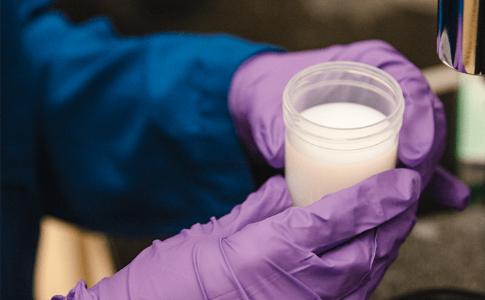
Batteries

Stored Power

Researchers are working on innovative energy storage systems—and discovering new potential in established technologies.

Evonik Country

USA: Endless opportunities

The USA is a pioneer when it comes to important future technologies—and that’s one reason why it’s Evonik’s second home.

ELEMENTS Newsletter
Get fascinating insights into the research Evonik is conducting, and its social relevance, by subscribing to our free newsletter.